The semiconductor industry is a high-stakes battleground where the smallest advancements in process technology can shift the balance of power. Intel’s 18A process isn’t just another incremental upgrade—it’s a daring move to reclaim technological supremacy from TSMC and redefine the future of chip manufacturing.
Set for high-volume production in the second half of 2025, Intel 18A (1.8nm-class) introduces cutting-edge RibbonFET transistors and PowerVia backside power delivery, technologies designed to boost performance, reduce power consumption, and outmaneuver competitors. With a 10% efficiency gain per watt over previous generations, 18A is Intel’s most advanced node yet, but the real question remains—can it leapfrog TSMC’s 2nm (N2) process?
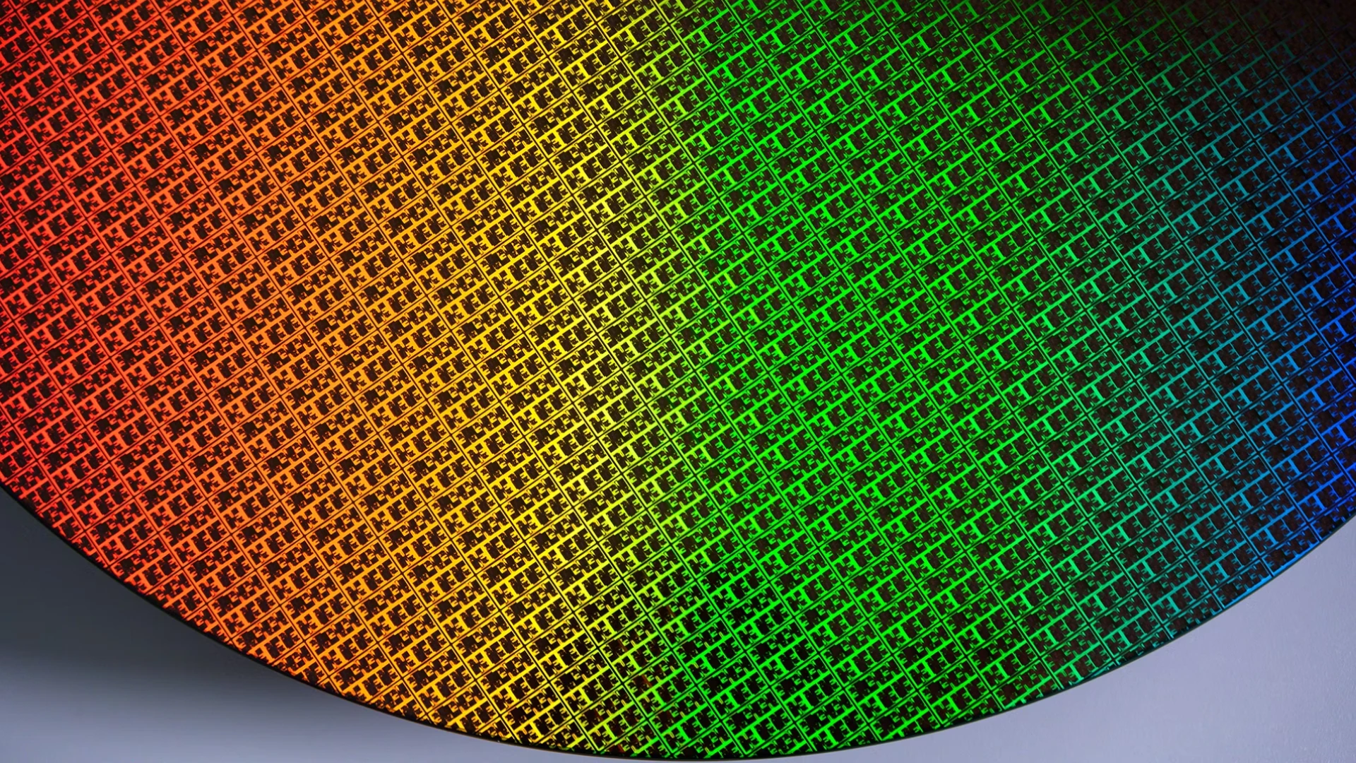
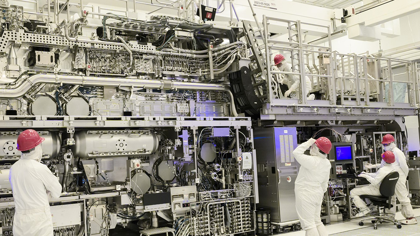
Images: Intel.com
A Billion-Dollar Gamble for the Future
For Intel, 18A isn’t just about making better chips—it’s a fight for survival and dominance. The semiconductor industry rewards innovation, but it also punishes failure brutally. Over the past decade, TSMC has cemented itself as the foundry of choice for giants like Apple, Nvidia, and AMD, leaving Intel struggling to keep up. 18A is Intel’s opportunity to break free from that losing streak and make a statement: “We’re back.”
Unlike previous nodes, 18A isn’t just for Intel’s own processors—it’s also a strategic play for foundry customers. AWS and Microsoft have already signed on, marking a shift in industry confidence. If Intel delivers on its promise, it could threaten TSMC’s iron grip on advanced semiconductor manufacturing.
Intel 18A vs. TSMC 2nm: Who Comes Out on Top?
Why Intel Could Win:
- Unmatched Performance: TechInsights’ latest research suggests Intel 18A is the highest-performing 2nm-class node, beating both TSMC and Samsung in raw speed.
- PowerVia: A Game-Changer: Intel’s backside power delivery tech reduces power loss and increases performance, something TSMC won’t implement until 2026 or later.
- Lower Costs? If Intel keeps pricing competitive, they could lure customers away from TSMC, whose $30,000 per wafer pricing is raising eyebrows across the industry.
- Government Support & CHIPS Act: Intel benefits from massive U.S. subsidies, making it a preferred choice for companies looking to reduce reliance on Taiwan-based TSMC.
Why TSMC Might Still Hold the Crown:
- Industry Trust & Reliability: TSMC is the gold standard in foundry manufacturing. Even if 18A is impressive, convincing Apple, Nvidia, and Qualcomm to switch won’t be easy.
- Better Density & SRAM Efficiency: TSMC’s 2nm has higher transistor and SRAM density, making it better suited for AI and datacenter workloads.
- Proven Yield & Mass Production: TSMC has a long history of delivering on schedule. While Intel’s yield reports are improving, mass production at scale is another challenge entirely.
The Road Ahead: Can Intel Deliver?
If Intel can execute on time, demonstrate high yields, and price 18A competitively, they might finally break TSMC’s stranglehold on the industry. However, TSMC isn’t standing still—its 2nm production begins in late 2025, and its dominance in mobile and AI chips means Intel has an uphill battle.
This isn’t just a race to 2nm-class supremacy. This is a battle for the future of computing. Will Intel 18A be the breakthrough that reshapes the industry, or just another near miss in the company’s long fight to regain dominance?
One thing is certain: the semiconductor wars are far from over.
Intel 18A vs. TSMC 2nm (N2)
| Factor | Intel 18A | TSMC 2nm (N2) | Winner? |
|---|---|---|---|
| Performance | Highest performance in the 2nm class (per TechInsights) | Strong but behind Intel 18A | Intel 18A |
| Power Efficiency | Expected to be competitive, but no confirmed lead | Industry leader in efficiency (TechInsights) | TSMC N2 |
| Density | 2nd place among 2nm-class nodes | Highest transistor and logic density | TSMC N2 |
| SRAM Density | ~32 Mb/mm² | ~38 Mb/mm² (TSMC leads in memory efficiency) | TSMC N2 |
| Backside Power Delivery (PowerVia) | Yes – first to implement in 2025 | No – TSMC delaying it to A16 in 2026-2027 | Intel 18A |
| Yield | Initial concerns about 10%, but multiple sources claim it’s much better | Early reports show strong SRAM yields (>80%) | Too early to call |
| Pricing | Competitive – may undercut TSMC’s high wafer cost | $30,000 per wafer (very expensive!) | Intel 18A |
| Customer Adoption | AWS & Microsoft have signed deals | Apple & Nvidia remain committed, but may delay adoption due to cost | TSMC N2 |
Why Intel 18A Could Disrupt TSMC
- Backside Power Delivery Gives Intel an Edge
- Intel is the first to introduce backside power delivery (PowerVia), improving performance and efficiency.
- TSMC won’t have it until 2026 or later, which means Intel could take the performance crown in 2025.
- TSMC’s Pricing Problem
- At $30,000 per wafer, TSMC’s 2nm is much more expensive than previous nodes.
- If Intel prices 18A competitively, it could lure customers away from TSMC.
- Growing Foundry Confidence in Intel
- AWS and Microsoft have committed to using 18A for AI and datacenter applications.
- If Intel delivers high yield and consistent production, it could attract more major clients.
- Government & CHIPS Act Support
- Intel benefits from U.S. government backing, making it a more viable option for companies looking to diversify production away from Taiwan.
Why TSMC Still Holds the Advantage
- Market Trust & Customer Base
- Apple, Nvidia, AMD, and Qualcomm are deeply integrated into TSMC’s ecosystem.
- Even with higher costs, TSMC still offers the most reliable production.
- Superior Transistor Density & SRAM Efficiency
- TSMC’s SRAM density is higher (38 Mb/mm² vs. Intel’s 32 Mb/mm²), which matters for AI and datacenter workloads.
- Higher logic density means better area efficiency for most chips.
- Yield & Production Experience
- TSMC has a long track record of delivering cutting-edge nodes at scale.
- Even if Intel 18A has good yield, TSMC has proven it can mass-produce high-quality wafers reliably.
Final Verdict: Does Intel 18A Leapfrog TSMC?
- In performance? ✅ Yes, Intel 18A leads.
- In efficiency? ❌ No, TSMC N2 is more power-efficient.
- In density? ❌ No, TSMC N2 is still the densest.
- In pricing? ✅ Yes, TSMC’s high cost gives Intel an opportunity.
- In customer adoption? ❌ Not yet, TSMC still dominates.
- In innovation? ✅ Yes, Intel’s PowerVia is a first.
Conclusion: Intel 18A is a serious challenger, but it won’t dethrone TSMC overnight.
- Intel could take the lead in high-performance computing (HPC), AI, and datacenters.
- TSMC still dominates in efficiency, density, and overall market trust.
- If Intel 18A delivers on yield and cost advantages, it could gain significant market share.
Intel isn’t leapfrogging TSMC just yet, but it has a real shot at disrupting the foundry market in 2025-2026.
Intel’s 18A Process: A New Era for Chipmaking?
The 18A Advantage: RibbonFET and PowerVia
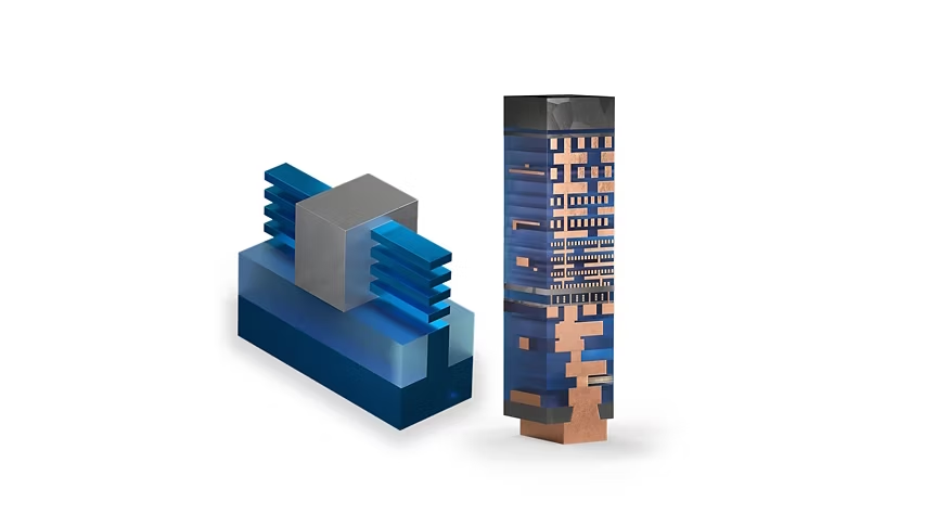
Intel’s 18A process uses two key technologies: RibbonFET and PowerVia. RibbonFET is Intel’s version of gate-all-around transistors. Think of it like this: traditional transistors have the gate on one side, but RibbonFET wraps the gate all the way around the channel, like a ribbon. This gives better control over the current, meaning more performance with less power.
PowerVia changes how power gets to the transistors. Instead of coming from the top, it comes from the back. This frees up space on the front for more transistors and makes the connections shorter, which also improves performance. It’s like moving the power lines underground in a city – less clutter and more efficient.
18A vs. the Competition
The big question is: how does 18A stack up against the competition, especially TSMC? TSMC is currently the leader in advanced chip manufacturing. Intel aims to close the gap, and maybe even take the lead, with 18A.
Both Intel and TSMC are pushing the limits of physics. They’re both working on 2nm-class processes. It’s a race to see who can get there first and who can make the best chips. The winner will likely dominate the market for a while.
What 18A Means for You
18A isn’t just about numbers and nanometers. It affects the devices we use every day. Faster processors mean smoother gaming, quicker video editing, and more powerful AI. More efficient chips mean longer battery life in laptops and phones. 18A could lead to a new generation of devices that are faster, more powerful, and more efficient.
The 18A Timeline
Intel has a clear roadmap for 18A. Panther Lake processors, designed for client computers, will be the first to use this technology. They’re expected to launch in the second half of 2025. High-volume production of 18A is planned for the first half of 2026. This timeline is crucial for Intel to stay competitive. Delays could mean falling behind.
18A’s Impact on the Industry
18A could shake up the entire semiconductor industry. If Intel succeeds, it will put pressure on TSMC and other chipmakers. This competition is good for consumers because it drives innovation and lowers prices. It’s like the car industry – competition leads to better cars at better prices.
Key 18A Features at a Glance
| Feature | Description |
|---|---|
| RibbonFET | Intel’s gate-all-around transistor technology for improved performance and power efficiency. |
| PowerVia | Backside power delivery network for increased transistor density and better signal routing. |
| Target Applications | Client computers, data centers, and other high-performance devices. |
| Timeline | Panther Lake launch expected in H2 2025; high-volume production in H1 2026. |
Key Takeaways
- Intel 18A will enter mass production in late 2025 with improved power efficiency
- The process combines three major technological breakthroughs in chip manufacturing
- External foundry customers can access Intel’s most advanced node technology
Intel 18A Process Technology Overview
Intel’s 18A process represents a major advancement in semiconductor manufacturing, featuring 1.8nm-class technology with RibbonFET transistors and PowerVia backside power delivery. The technology aims to start high-volume production in late 2025.
Technological Advancements and Innovations
RibbonFET architecture marks Intel’s first gate-all-around transistor design. This structure enables better control of current flow and reduces power leakage compared to previous FinFET designs.
PowerVia technology introduces backside power delivery, separating the power delivery network from the signal network. This separation increases signal integrity and power efficiency.
The combination of RibbonFET and PowerVia creates a more efficient chip architecture with improved performance per watt metrics.
Comparative Analysis with Other Process Technologies
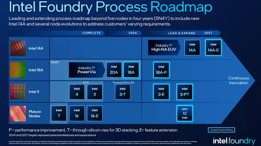
Intel 18A follows the company’s aggressive process roadmap after Intel 3, Intel 4, and Intel 20A nodes.
TSMC’s N2 technology (2nm-class) will compete directly with Intel 18A in the foundry market. Both technologies target production in the second half of 2025.
The 18A process builds upon improvements from Intel’s previous nodes while introducing new architectural changes for enhanced performance.
Impact on Business and Foundry Customers
Intel Foundry Services will offer 18A technology to external customers as part of their IDM 2.0 strategy.
The process technology strengthens Intel’s position in the foundry market, providing customers access to leading-edge manufacturing capabilities.
Early customer sampling of 18A-based Panther Lake processors demonstrates Intel’s progress in development and manufacturing readiness.
Production and Manufacturing Details
High-volume manufacturing is scheduled for the second half of 2025.
Intel’s fabrication facilities are being upgraded to support 18A production requirements.
The process integrates with Intel’s five nodes in four years (5N4Y) manufacturing strategy.
Future Developments and Roadmap
Intel has announced plans for specialized node evolutions of 18A to address specific market needs.
The company continues development of Intel 14A as the next node following 18A.
Integration of 18A technology will begin with Panther Lake processors, showcasing the capabilities of this advanced manufacturing process.